The Atomic Force Microscope (AFM) is a scanning probe imaging instrument that allows 3D reconstruction and topography measurements of samples. It also allows the investigation of physical properties of materials. The typical contact radius of an AFM probe is in the order of few nanometres but operation employing the colloid probe technique involves a sensor which replaces the tip with a micron sized bead.
Horizontal resolution, limited by the contact radius of the probe, is of the order of a few nanometres, while vertical resolution can be routinely attained in the sub-nanometre domain. Its sensors can detect interaction forces down to 10-12 Newtons.
The AFM application fields range from material science to electrostatic, magnetic and chemical force microscopy and also DNA imaging and cellular nanomechanics.
The facilities at ANFF-Q cover all major application domains of atomic force microscopy. Along with the MFP-3D, Cypher (Asylum Research/Oxford Instruments) and NanoWizard® II (JPK), ANFF-Q hosts WITec alpha300, a system capable of integrating AFM pulsed force microscopy, confocal Raman spectroscopy and scanning near-field optical microscopy (SNOM).
Examples of use
Block-copolymers Characterisation of block-copolymers designed to encapsulate bone prostheses. AFM can be used to create 3D topographic images of the polymer film, to perform roughness analysis, to generate adhesive force maps and to measure interaction force curves or phase images obtained in air or/and fluid.
Microfluidic devices For microfluidic devices the feature dimensions and surface characteristics are critical to the device design. AFM can provide 3D and 2D topographic images of a device together with cross sections and roughness analysis.
Patterned glass substrates Patterned glass substrates are fabricated for controlled cell deposition and culture. AFM can be used to create topographic images of the patterned substrate and adhesive force maps of interactions between the cells and the desired areas.
Nano-mechanical measurements AFM can perform fast, quantitative nano-mechanical measurements of materials ranging from HOPG to DNA. For more information, please refer to the Microscopy and Analysis supplement.
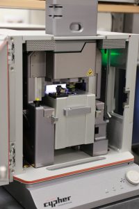
Asylum Research Cypher AFM
Purpose: A purpose built AFM in a dedicated enclosure to investigate surface nanomechanics and topography.
Material systems: Organic, inorganic and biological.
Scale/volume: 30 µm x 30 µm topographical map on a 15 mm diameter substrate
Specifications/resolution:
Kelvin probe force microscopy (KPFM), high voltage piezoresponse force microscopy (HV-PFM), scanning tunnelling microscopy (STM), AM-FM viscoelastic mapping mode: quantitatively maps both the storage modulus (elastic response) and loss modulus or loss tangent (viscous response) with nanoscale resolution.
The Park Systems NX20 is a high-performance Atomic Force Microscope (AFM) designed for large-sample inspection in semiconductor and MEMS applications. It offers precise topography measurements with low noise and supports multiple scanning modes, including True Non-Contact™ Mode to preserve probe life. The system features automated, recipe-driven measurements for efficient and reproducible data acquisition. It is widely used for surface characterization, failure analysis, and 3D profiling of advanced devices.
Material systems: Organic, inorganic and biological.
Scale/volume: 30 µm x 30 µm topographical map on a 15 mm diameter substrate
Specifications/resolution:
Kelvin probe force microscopy (KPFM), high voltage piezoresponse force microscopy (HV-PFM), scanning tunnelling microscopy (STM), AM-FM viscoelastic mapping mode: quantitatively maps both the storage modulus (elastic response) and loss modulus or loss tangent (viscous response) with nanoscale resolution.
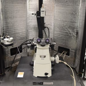
AFM built on a Nikon inverted microscope. Used to investigate surfaces materials and take quantitative nanoscale measurements.
Material systems:
Organic, inorganic and biological.
Scale/volume: 90 µm x 90 µm topographical maps.
Specifications/resolution:
Sub-nanometre resolution in Z, Kelvin force probe/adhesion and stiffness maps, conductivity maps and single molecule spectroscopy, viscoelastic mapping, magnetic force mapping.
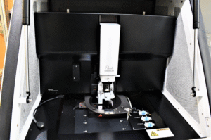
A large sample stage AFM in a dedicated enclosure to investigate nanomechanical and nanoelectrical properties including topography and roughness analysis.
Material systems:
Organic, inorganic and biological.
Scale/volume:
100 µm x 100 µm topographical map; can accommodatesmall as well as large samples including analysis of 8 inch wafers.
Specifications/resolution:
ScanAsyst™, PeakForce™ Tapping, Contact Resonance, PeakForce™ QNM – quantification of nanomechanical properties, Kelvin probe force microscopy KPFM), PeakForce™ TUNA, DataCube TUNA – nanoelectrical measurements in Air and liquid environment with nanoscale resolution.
NanoWizard® 4 XP BioScience atomic force microscope (BioAFM)
Examples of use:
PeakForce Tapping or QI Advanced Imaging modes for easy surface imaging. Dedicated design of NanoWizard 4 XP provides highest mechanical and thermal stability, which provides great advantage on live cell surface imaging and mechanic property measurement. Electrochemistry measurements. Mechanical property test with temperature control. Correlate optical images with AFM images. Colloidal probe fabrication.
Purpose:
NanoWizard 4 XP AFM combines atomic resolution and a large scan range of 100 µm in one system. It is designed to provide highest mechanical and thermal stability on inverted optical microscopes during long term experiments on samples ranging from single molecules to living cells and tissues. Highest flexibility and upgradeability with a broad range of modes and accessories
Material systems:
Organic, inorganic and biological.
Scale/volume:
Scan size 100 × 100 × 15 µm3 with the capability to increase z range up to 100 µm.
Specifications/resolution:
Sub-nanometre resolution in Z axis, fluid cell, temperature and gas control for biological samples, Celhesion module (piezo crystal 100 µm in Z), optical/AFM image overlay and electrochemical unit.
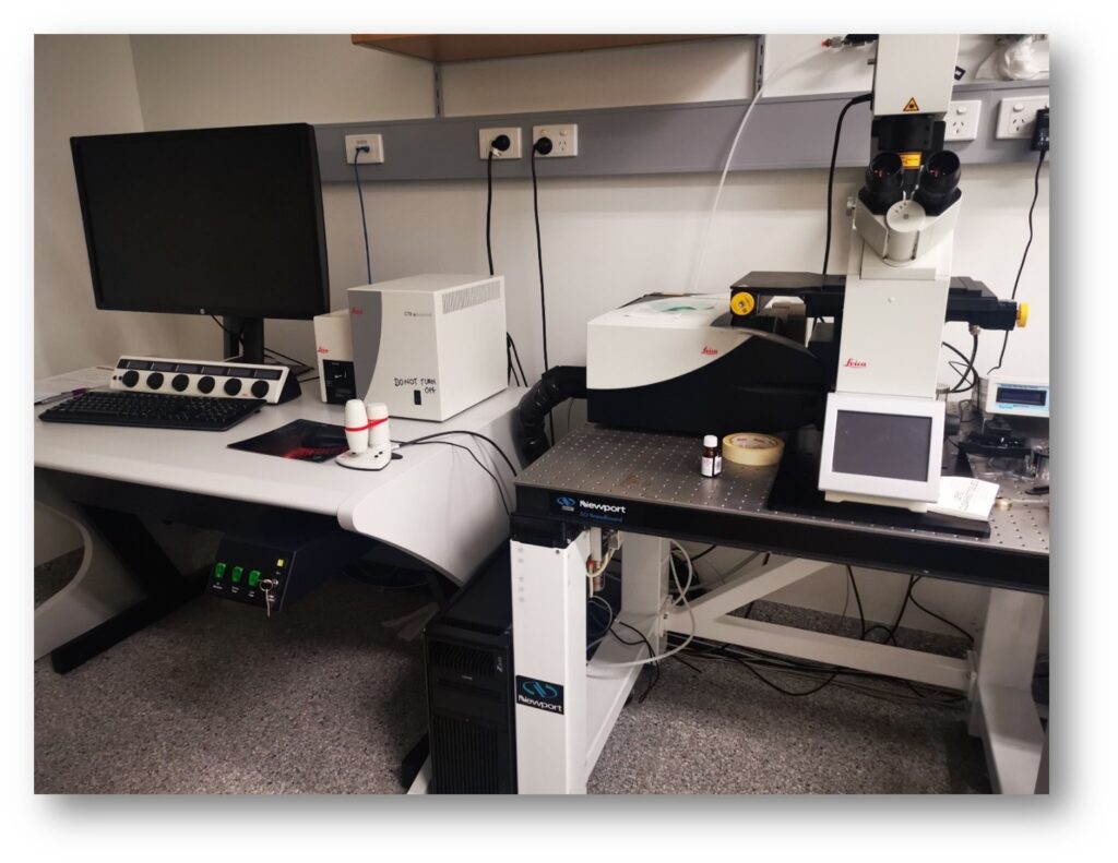
A confocal Raman AFM SNOM (scanning near-field optical microscopy) system with digital pulse force module. Capable of obtaining information from the sample surface as well as chemical maps.
Material systems:
Organic, inorganic and biological.
Scale/volume:
90 µm x 90 µm topographical/Raman chemical map.
Specifications/resolution:
Sub-nanometre resolution in Z, 532 and 633 nm laser source, stiffness, adhesion maps, 300 nm Raman spot size and 25 µm, 50 µm and 100 µm pinhole.
Confocal laser scanning microscopes create 3D images by sequentially scanning samples point by point, or multiple points at once, then assembling this pixel information into an image. As a result you can acquire optical sections with high contrast and high resolution in x, y and z. Confocal microscopes are used in biomedical research and surface analysis in material science applications, offering extraordinary precision in 3D imaging and examination of subcellular structures and dynamic processes.
The facilities at ANFF-Q cover all major application domains of confocal laser scanning microscopy. At ANFF-Q, we have three state-of-the-art confocal scanning microscopes: Leica SP8 with White light laser and Zeiss LSM 710.
Confocal module with patented filter-free spectral Leica SP detector for up to five individually regulatable channels. Highly efficient spectral separation by unique prism design. Leica patented Acousto-Optical Beam splitter (AOBS) provides optimal spectral flexibility with up to 8 laser lines simultaneously. Highly synergistic in combination with prism, Leica SP detector and White Light Laser. Unique selectivity for optimal image contrast, undistorted recording of emission spectra ideal dye separation and exquisite signal efficiency resulting in maximum sample viability.
Leica HyD detector provides super-sensitive photon detection making it ideal for low light and live cell imaging. Thanks to its very low dark noise it produces brilliant imagery rich in contract and fidelity for finest details.
The Leica SP8 has two laser lines (405nm, 442nm) and the White Light Laser (WLL). The (WLL) is a fully tunable super continuum laser with up to eight simultaneously usable lines in the range of 470 – 670 nm for maximal spectral flexibility in combination with AOBS and SP detector. In conjunction with internal HyDs time gated detection is enabled.
Examples of use:
The Leica SP8 is suitable for imaging a wide variety of samples, including live cells, biopolymer and polymer films, food chemistry materials, and agricultural products. It supports advanced imaging techniques such as tile scanning, time-lapse series, and photobleaching experiments like Fluorescence Recovery After Photobleaching (FRAP). The system also enables high-quality 3D imaging across diverse sample types.
With its resonant scanner, the SP8 significantly enhances imaging speed, operating at an approximate line frequency of 16,000 Hz (bidirectional) and achieving up to 28 frames per second at a 512 × 512 resolution.
Purpose:
A confocal laser scanning microscope designed for the precise examination of a broad range of samples, including those related to materials science, food chemistry, agriculture, microfluidic devices, bioengineering, energy storage, and nanotechnology.
Material systems: Organic, inorganic and biological (auto fluorescent or stained samples).
Scale/volume: Scan field: 20 mm diagonal maximum.
Specifications/resolution:
Built on an inverted microscope; X-Y-Z motorized stage; maximum image resolution is 64 megapixels; spectral detection of 400 to 700 nm; lasers: 405 nm and 442nm; white light laser for 470-670nm; Z range of up to 300 µm; a temperature stage of up to 50 degrees; incubation chamber with 35mm dish insert; and has time series measurements. Our Leica SP8 has four air objectives (2.5x, 10x, 20x and 40x), one water immersion objective (40x) and one (63x) oil immersion objectives.
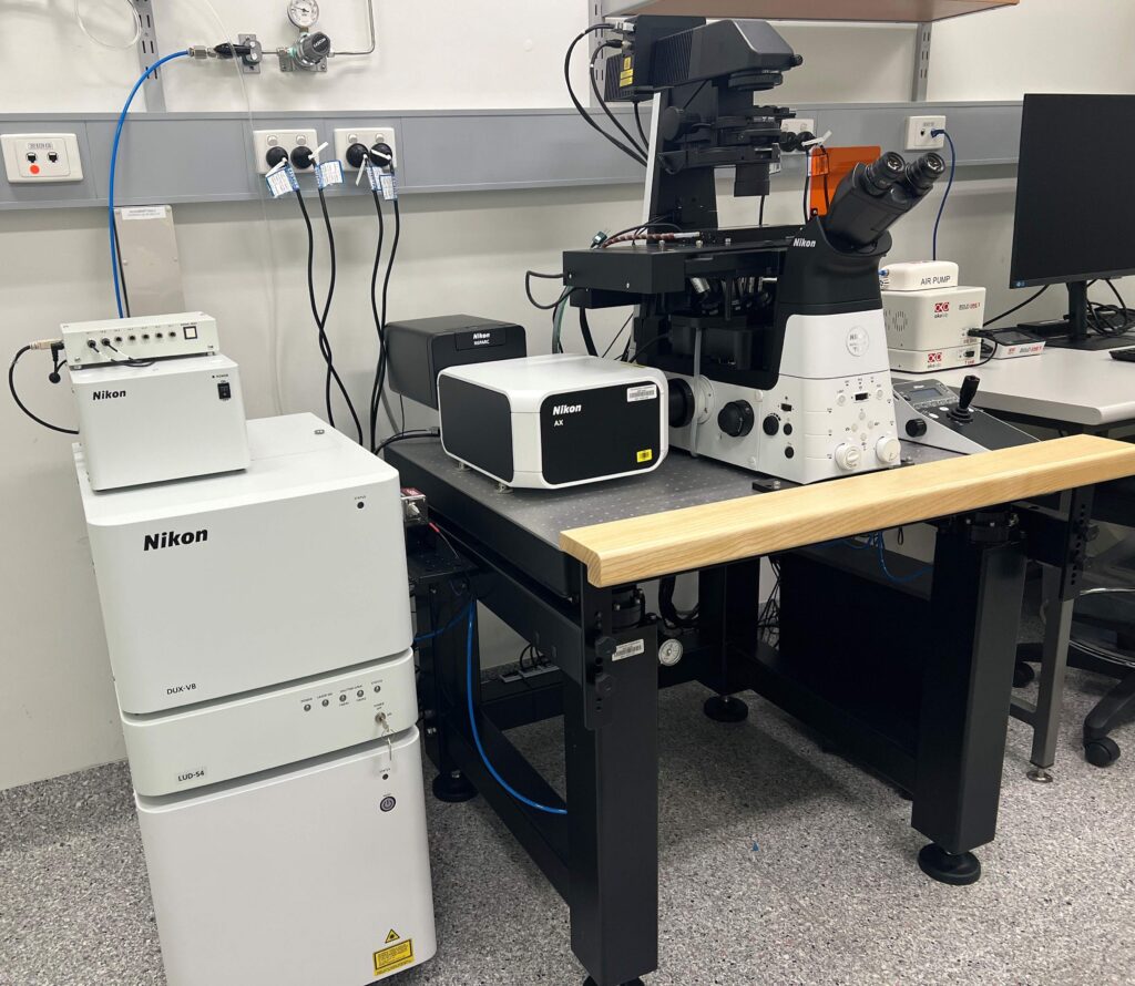
Nikon AXR Confocal Laser Scanning Microscope with NSPARC Detector
The Nikon AXR confocal laser scanning microscope features the advanced NSPARC detector, delivering ultra-sensitive single-photon detection with exceptionally low noise for clear, high-contrast images. Equipped with multiple laser lines: 405 nm, 488 nm, 561 nm, 638 nm, and 730 nm. This system offers broad spectral flexibility, enabling excitation of a wide range of fluorophores from visible to near-infrared wavelengths.
The microscope supports both resonant and Galvano scanning modes, providing versatile imaging options for high-speed live-cell experiments as well as high-resolution structural analysis. Integrated with Nikon’s powerful imaging software, the AXR facilitates multi-channel imaging, multipoint, time-lapse acquisition, tile imaging, photostimulation (such as FRAP), and detailed 3D reconstructions.
Examples of Use:
The Nikon AXR is ideal for imaging a variety of samples, including live cells, thick tissue sections, polymer films, and complex biological specimens. It supports tile scanning, volume imaging, time series, and bleaching experiments. The resonant scanner enables rapid imaging speeds while maintaining high resolution and sensitivity.
Purpose: Confocal laser scanning microscope designed for precise imaging across diverse fields including cell biology, neuroscience, developmental biology, plant science, immunology, and materials research.
Material Systems: Organic, inorganic, and biological samples (both auto fluorescent and stained).
Scale/Volume: Scan field: up to 25 mm diagonal
Specifications/Resolution:
The system is built on an inverted microscope and X-Y-Z motorised stage. Detector sensitivity from 400nm to 900 nm.
Lasers: 405 nm and 488nm, 561nm, 638nm and 730 nm; a stage top incubator heating up to 60 degrees with 35mm dish, glass slide and well plate insert.
Resonant and Galvano scanners for flexible speed and resolution. Temperature control and incubation options available. Supports multi-dimension acquisition, including multi-channel, time series, multipoint, z-stack and tile acquisition.
Objectives: Four air objectives (4x, 10x, 20x and 40x), one silicon oil immersion objective (25x), and two oil immersion objectives (60x, and 100x).
Key Features:
Fast large-tissue scanning – A 25 mm field of view enables scanning of large samples with fewer frames, increasing throughput and efficiency.
Super-resolution – Achieve super-resolution imaging without additional sample preparation by leveraging the high sensitivity of the NSPARC detector.
Cellular dynamics – The ultra-fast resonant scanner captures dynamic cellular events at speeds up to 720 frames per second (fps).
Sensitive samples – The ultra-low-noise, high-sensitivity NSPARC detector requires minimal laser excitation, preserving delicate samples and reducing photodamage.
Volume imaging – Combining the ultra-fast resonant scanner with the low-noise NSPARC detector enables rapid capture of large 3D volumes.
Multiplexing/multichannel imaging – Equipped with 5 laser lines, the system produces accurate spectral signatures that improve unmixing and separation of multiple fluorophores in complex staining experiments.
A confocal laser scanning microscope (CLSM) combines high-resolution optical imaging with depth selectivity which allows us to do optical sectioning. This means that we can view visual sections of tiny structures that would be difficult to physically section (e.g. embryos) and construct 3D structures from the obtained images. It scans a sample sequentially point by point or multiple points at once, using a focused laser beam to allow for 3D reconstruction. The pixel information is assembled into an image.
In a conventional microscope you can only see as far as the light can penetrate whereas a confocal microscope images one depth level at a time. As a result you can acquire optical sections with high contrast and high resolution in X, Y and Z.
The Zeiss LSM 710 confocal laser scanning microscope has a high signal-to-noise ratio enabling brilliant imaging even in deep-lying tissue layers. Users can capture high-resolution images of fluorescent structures in living animals and thick tissue specimens, 3D structure of cells and also can perform time series experiments to see changes in the sample. It also allows recording of up to five fluorescence signals in the non-descanned mode. It is a perfect choice for neurobiologists, developmental biologists, immunologists and plant biologists as well as material scientists.
Examples of use:
CLSM can be used for imaging different samples ranging from live cells to biopolymer/polymer films. It can be used to understand cell-nanoparticle interaction to changes in microstructure of plant tissue at different maturity stages. It can also be used to perform Fluorescence recovery after photo-bleaching (FRAP), Fluorescence resonance energy transfer (FRET), different time series as well as bleaching experiments. One can obtain 3D images and tile scans on a range of samples.
Purpose:
Confocal laser scanning microscope for the precise examination of complex biological systems.
Material systems:
Organic, inorganic and biological (autofluorescent or stained samples).
Scale/volume:
Scan field: 20 mm diagonal maximum.
Specifications/resolution:
Built on an inverted microscope; X-Y-Z motorized stage; scan resolution from 4 x 1 to 6 144 x 6 144 pixels; spectral detection of 400 to 700 nm; four lasers: 405 nm, Argon laser 458/488/514 nm, 561 nm and 633 nm; Z range of up to 300 µm; a temperature stage of up to 60 degrees; incubator for 6, 12, 24 and 96 wells; and has time series measurements. Our LSM 710 has three air objectives (5x, 10x and 20x), one water immersion objective (40x) and two (63x and 100x) oil immersion objectives.
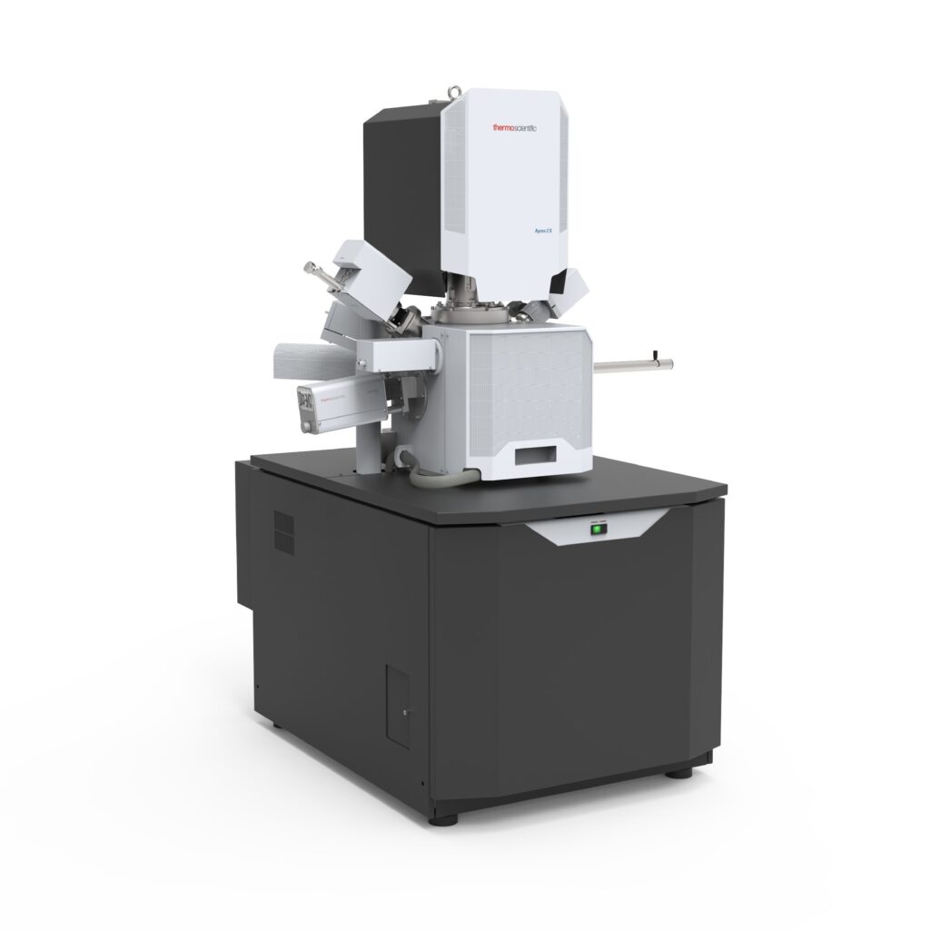
Scanning Electron Microscope (SEM), Thermo Fisher Scientific Apreo 2S
*NOT an ANFF-supported tool, however, access is available upon completion of training. Please contact the tool owner listed below for further details.
The Apreo 2S scanning electron microscope (SEM) is a state-of-the-art system offering sub-nanometer resolution and advanced imaging capabilities. It is ideally suited for high-resolution surface imaging, compositional contrast, and analytical techniques such as Energy Dispersive Spectroscopy (EDS), with excellent performance even at low accelerating voltages.
Examples of use:
High-resolution imaging of nanostructures
Surface and compositional analysis of materials
Elemental analysis using EDS
Semiconductor device inspection and failure analysis
Purpose:
Used for detailed imaging and characterisation of materials at the micro- and nanoscale, enabling researchers to study morphology, composition, and structure with high precision.
The KLA P-7 can be used to measure film stress (tensile or compressive) by measuring changes in the radius of curvature before and after a film has been deposited. This system requires a patterned step to measure step height. If one does not exist consider a non-contact method such as ellipsometry.
The KLA P-7 uses a stylus tip to measure step height, waviness, and roughness of samples. It offers complete high-resolution 2D &3D analysis of surface topography in a versatile platform. The system is capable of scanning up to 150 mm wafers with high resolution. It has adjustable scan speeds and stylus force settings which allow for flexibility with any surface to be measured.
Purpose:
The KLA P-7 Stylus Profiler (contact measurement) nanometre-level film, step and surface measurements.
Material systems:
Standard photoresists, semiconductors, soft and hard materials with vertical step height up to 1 mm in thickness.
Limitations on materials:
No uncured SU8 and photoresists, no soft material that might stick to the stylus.
Limitations substrate size and thickness:
No samples greater than 150 mm in diameter or smaller than 10mm x 10mm
Equipment Configuration :
Step height: Nanometers to 1000µm
Sample chuck: 6 inches
Scan speed: 2-25000 um/s
Low force with constant force control: 0.03 to 50 mg
Scan full diameter of the sample without stitching
Video: 5MP high-resolution colour camera
Arc correction: Removes error due to arc motion of the stylus
Production capability: Fully automated with sequencing, pattern recognition and SECS/GEM
Maximum Range: 1000 microns
Stylus Tip Radius: 2 and 5 microns
Applications
Step height: 2D and 3D step height
Texture: 2D and 3D roughness and waviness
Form: 2D and 3D bow and shape
Stress: 2D and 3D thin-film stress
JEOL IT-300 scanning electron microscope (SEM)
The JEOL IT‐300 is the latest generation tungsten filament SEM with an advanced EOS (electron optic system) capable of imaging with a minimum of 3 nm resolution at 30 kV. This system is equipped with both the secondary and backscattered electron detector for obtaining both topographical and elemental information on the sample material. The IT-300 system is also equipped with variable pressure apparatus that will allow users to image more insulated samples than traditional SEMs. In addition, the JEOL IT‐300 comes with a large chamber and a fully automated 5 axis eucentric stage that will allow users to image a full 6” Si wafer without the need for breaking up their wafers. This tool is located in class 1 000 cleanrooms, allowing users to rapidly develop new processes in the cleanroom without the risk of exposing samples to dust and white light environments.
JEOL Sputtering System to coat samples
A JEOL platinum sputtering system is also available to coat samples before analysis.
Purpose:
Metrology tool to allow process development during the etching and other fabrication processes using high magnification and resolution images
Material systems:
Any, as long as the samples are dry and don’t outgas. Nanoparticles must be embedded or fixed onto a surface.
Scale/volume:
Single and/or multiple sample/system up to 6” wafers.
Specifications/resolution:
Max stated resolution is 3 nm however realistic resolutions depend on the sample material and the way the sample is prepared and mounted.
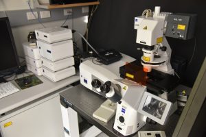
ANFF-Q’s Nikon Eclipse Ti-U inverted microscope is a phase contrast and fluorescent imaging microscope equipped with NIS-Elements Advanced Research software, allowing our users to control all microscope and camera functions. The Eclipse Ti-U uses Nikon’s CFI60 optical system and a wide choice of objectives for bright field, fluorescence, phase contrast and differential interference contrast (DIC). Combined with NIS-Elements imaging software, the Ti-U enables diverse image acquisition and analysis methods such as multi-dimensional time-lapse imaging to acquire temporal and spatial information of fast, dynamic live cell processes. This microscope is equipped with the Phantom V9.1 high speed colour camera, from Vision research, has maximum speeds of 1 000 frames per second with a full resolution of 1 632 x 1 200 pixels and 150 000 frame per second at the lowest resolution of 96 x 8 pixels. The Phantom V9.1 has a vertical resolution of 1 200 pixels. It is most probably because of its high vertical resolution that the Phantom cameras are the most popular cameras in the field of micro-fluidics. Phantom V9.1 camera has a higher internal memory, which is useful for making the relatively large movies (up to 30 to 60 sec) required for most of the microfluidic applications.
Examples of use
Image acquisition and analysis of dynamic live cell processes.
Purpose:
Used for 2D and 3D imaging and analysis.
Scale/volume:
Maximum stage size is 310 mm x 300 mm.
Specifications/resolution:
Five air objectives (5x, 10x, 20x, 40x and 60x) and one oil immersion objective (100x). Five filters (405 nm, 488 nm, 560 nm, 585 nm, 632 nm). A monochrome digital camera up to 1 280 x 1 024 pixels and 50 frames per second.
SCI FilmTek 2000M is a breakthrough in thin film metrology technology. FilmTek 2000M combines a fibre-optic spectrophotometer with revolutionary material modelling software to provide an affordable and reliable tool for the simultaneous measurement of film thickness, index of refraction, and extinction coefficient. FilmTek 2000M provides unmatched accuracy, ease of use, and analytical power in a fully integrated package. Ideally suited for patterned device wafers, the FilmTek 2000M allows for measurement spot sizes as small as 2 µm.
Examples of use:
Measurement of:
Multiple layer thicknesses
Indices of refraction [ n(ƛ) ]
Extinction (absorption) coefficients [ k(ƛ ) ]
Energy band gap [ Eg ]
Constituent and void fraction
Surface roughness
Purpose:
Characterise thin film properties.
Material systems:
Transparent films.
Scale/volume:
Small sample to 6” wafer.
Specifications/resolution:
Film thickness range: 3 nm to 350 µm (5 nm to 150 µm is standard). Film thickness accuracy: ±1.5 Å Spectral range: 240 nm to 950 nm is standard. FilmTek 2000M measurement spot size: 2 µm to 50 µm Pattern recognition (Cognex)
SurPASS electrokinetic analyser for solid surface analysis
The SurPASS instrument by Anton Paar is an electrokinetic analyser for solid surface analysis and deals with the properties and behaviour of surfaces of macroscopic solids.
Examples of use
The zeta potential is an indicator for charge formation at the solid-liquid interface. The SurPASS is an analytical instrument for research and development which is used in many fields of applications, e.g. membranes, biomaterials and semiconductors. Knowledge of the zeta potential is important to understand the behaviour of solid materials in many technical and biological processes. Information provided by the SurPASS thus helps to efficiently modify material surfaces to fulfil certain conditions.
Purpose:
Surface charge measurement.
Material systems:
Membranes and filters, polymers and composites, semiconductors, biomaterials, synthetic and natural fibres and textiles, cosmetics and surfactants, mineral powders.
Scale/volume:
10 mm x 20 mm solid surfaces
Specifications/resolution:
Adjustable gap cell 20 mm × 10 mm, thickness <2 mm disks, clamping cell minimum 55 mm × 25 mm, thickness <30 mm, cylindrical cell particle size >30 µm.
The RC2 spectroscopic ellipsometer provides innovative new technology: dual rotating compensators, achromatic compensator design, advanced light source, and next-generation spectrometer design. The RC2 is a near-universal solution for the diverse applications of spectroscopic ellipsometry and Mueller matrix ellipsometry.
Purpose:
The RC2 ellipsometer determines information about thickness and optical properties (refractive index, extension coefficient) of thin films on substrate.
Material systems:
Organic, inorganic and polymers.
Scale/volume:
Handles 6 inch to below up to 1 inch wafers of flat or curved surface.
Specifications/resolution:
210 nm to 2500 nm wavelength range, CCD detector, automatic sample alignment, automated angle of incidence ranging from 45 degree to 90 degree, upto 200 mm diameter sample size
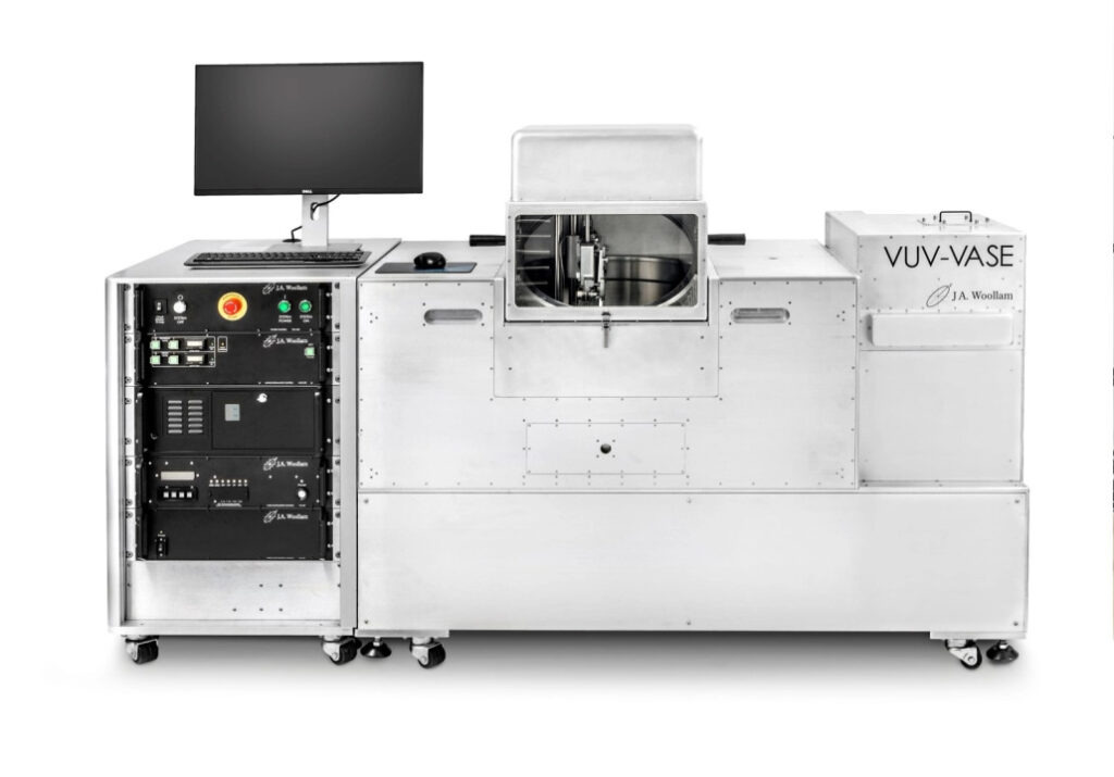
The VUV-VASE GEN-II by J.A. Woollam is a high-performance spectroscopic ellipsometer designed for advanced thin-film and optical material characterization. It covers a wide spectral range from the vacuum ultraviolet (<150 nm) to the near-infrared (~1700 nm), enabling precise analysis of ultra-thin films and high bandgap materials. The system supports large wafer mapping (up to 300 mm), uses nitrogen purge for accurate VUV measurements, and offers versatile modes including reflection, transmission etc. It is widely used in semiconductor lithography, optical coatings, and materials science research.
Example of use
Charaterising ultra-thin dielectric films for microelectronics
Determining optical constants of wide bandgap materials
Purpose:
To provide high-precision optical and thickness characterization of thin films and materials across a very broad spectral range. It is particularly valuable for semiconductor, nanotechnology, and materials research, where understanding optical properties at VUV wavelengths is critical for developing advanced devices and coatings.
The Zeiss AxioLab.A1 upright microscope features 5 position objective nosepiece, 4 position reflector turret, mechanical stage, 50 W halogen light for reflected light, reflector modules for bright field and dark field, binocular phototube with 50/50 split, enhanced contrast EC “Epiplan” HD objectives: 5x, 10x, 20x, 50x and 100x. The system also includes the AxioCam ICc1 colour camera (Fire Wire) and AxioVision software for image acquisition and module for Online and Interactive Measurement.
Examples of use:
Biological samples, MEMS, cytology and immunofluorescence.
The Zeta 300 is a multi-mode optical profiler packed with features. It is a fully integrated, metrology platform that can allows automatic data acquisition and analysis for very complicated structures. The system has four profiling modes:
ZFT mode gives very accurate multilayer film thickness measurement based on white light reflectometry.
ZDot mode is used to profile 3D structures, surface roughness, and resist step heights.
ZX and ZSI mode are vertical scanning and phase contrast interferometry capable of delivery sub nm precision measurement on step heights and polished surfaces.
Examples of Use:
Single and multilayer film thickness measurement, 3D profiling, CD measurement, surface roughness measurement, automated metrology and data analysis.
Purpose:
CD measurement and 3D profiling.
Material Systems:
Sample with surface reflectivity above 0.5%. Polymer film on Si wafer.
Scale/ Volume:
Maximum sample size = 6” substrate, 100 mm thick
Specifications/ Resolution:
White light imaging, interferometric, motorised stage Z resolution < 1 nm using interferometry modes Lateral resolution > 370 nm at 150 X
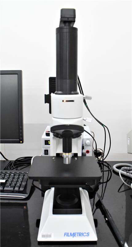
The Filmetrics F40-NSR Thin-Film Measurement System
The Filmetrics F40-NSR Thin-Film Measurement System is a high-precision reflectometry instrument designed for fast and non-destructive thin-film thickness analysis. Using spectral reflectance, it provides accurate measurement of transparent and semi-transparent films. Ideal for semiconductor, optical coatings, MEMS, and nanotechnology applications.
Examples of use
Thin film thickness measurement, refractive index determination, film uniformity mapping, optical coating characterisation
Purpose
To measure thin film thickness, refractive index, and uniformity using non-contact optical reflectometry
Material systems:
Dielectrics, semiconductors, photoresists, polymers, and transparent thin films
Scale/volume:
Spot size down to a few microns; compatible with wafers and substrates up to 200 mm
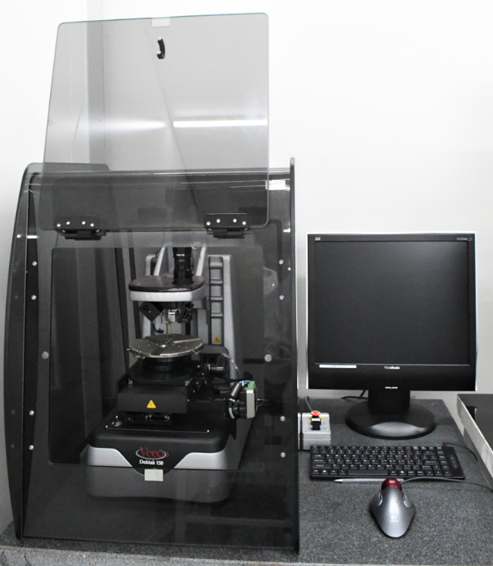
The Veeco Dektak Stylus Profilometer is a versatile surface measurement system designed for thin-film research and quality control. It provides high-resolution step height, thickness, and roughness measurements with reliable repeatability. Ideal for semiconductor, MEMS, optical coatings, and nanotechnology applications.
Examples of use
Film thickness measurement, step-height profiling, surface roughness characterisation, stress analysis.
Purpose
To measure and characterize film thickness, step height, and surface morphology
Material systems:
Metals, semiconductors, polymers, dielectrics, and thin-film composites
Scale/volume:
Accommodates samples up to 150 mm (6-inch wafers)
Specifications/resolution:
Measurement range: nanometers to hundreds of microns
Stylus force: adjustable (low force option for soft films)