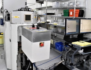
The Plasma-Therm Versaline DRIE system is an inductively coupled plasma (ICP) etch system for deep silicon etching using the Bosch process. The deep silicon etching (DSE) process alternates between deposition and isotropic etching in a chamber with an ICP configuration. A conformal polymer is deposited, and then the polymer is removed only from the horizontal surfaces, allowing isotropic etching during the next step. The deposition gas is typically C4F8 and the etching gas is commonly SF6.
The DSE technology has been developed to achieve extremely high aspect ratio features on silicon substrates. DSE provides:
High silicon (Si) etch rate
Good etch profile quality
Improved SOI (silicon on insulator) etch performance
Examples of use:
It is used for the development of:
Microelectromechanical systems (MEMS)
DRAM memory circuits
Purpose:
To create deep, often steep sided trenches and other structures in silicon wafers. To produce nanopatches for Bio-application.
Material systems:
Silicon only.
Scale/volume:
6 inch wafer.
Specifications/resolution:
Fast silicon etch rate 3 – 5 µm/min with a deep vertical wall. In addition, etching parameters can be adjusted to make different shapes. Gases: SF6, C4F8, argon and oxygen.
Model:
Plasma-Therm Versaline DRIE system
Site:
The University of Queensland
Location:
Class 10 000 cleanroom, Level 2E, AIBN (Bldg #75), St Lucia
The STS ICP Multiplex Etcher is a versatile plasma etching system designed for precise and uniform material removal in microfabrication processes. It uses Inductively Coupled Plasma (ICP) technology to achieve high etch rates and process control. This tool is used in research and industry for producing advanced semiconductor and MEMS devices.
Examples of use:
It is used for the development of:
Etching silicon wafers for MEMS devices
Defining microstructures for optical and photonic devices
Fabricating channels and features for microfluidic devices
Processing advanced semiconductor components requiring precise pattern transfer
Purpose:
To perform controlled plasma etching for microfabrication processes. It is used to create accurate and uniform features in semiconductor, MEMS, and microfluidic devices.
Material systems:
Silicon, Silicon carbide, Sapphire, Quartz and other materials (considered on requests)
Scale/volume:
6 inch wafer.
Specifications/resolution:
Etching parameters can be adjusted to make different shapes.
Available gases: SF6, C4F8, Ar, O2, Cl2, and BCl3.
The ADT 7100 precision dicing saw is used to cut substrates into individual chips or dice. It employs a high-speed spindle fitted with an extremely thin diamond blade to cut with high precision, semiconductor wafers, glass, ceramics and other types of materials. It is capable of processing up to 8 inch wafers.
The dicing machine runs at high power (2.4 kW), which makes this instrument capable of cutting hard and thick materials like bonded wafers.
Examples of use
ADT Model 7100 series is an industry leading platform designed for a variety of applications such as:
ceramic substrates and capacitors
automotive sensors
glass
glass on silicon
PZT
SAW filters
sensors and MEMS
LED and LED on PCB packages
package singulation (BGA, QFN)
LTCC
opto-electronic components
IC wafers
Purpose:
Dicing of silicon and other wafers.
Material systems:
Silicon, glass, germanium and III IV materials wafers.
Scale/volume:
Single wafer processing up to 8 inch size.
Specifications/resolution:
Saw blade minimal width of 20 µm with space resolution of 0.1 µm.
The DISCO 2H/6T is a high-precision wafer dicing saw designed for cutting semiconductor and MEMS wafers into individual chips. It offers excellent cutting accuracy, high-speed operation, and minimal chipping, even on thin or fragile wafers. This tool is widely used in semiconductor device fabrication, LED processing, and other microelectronic applications. Its reliable performance ensures consistent and precise wafer separation for advanced manufacturing.
Reactive ion etching (RIE) is a type of dry etching which uses chemically reactive plasma to remove material from substrates. ANFF-Q has two reactive ion etchers.
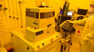
Oxford reactive ion etcher
Oxford Instruments PlasmaPro 80 Reactive Ion Etcher(RIE) is a compact, small footprint system offering versatile reactive ion etch solutions on one platform with convenient open loading. The etcher is a turbo-pumped RIE system with backside helium cooling dedicated to processes involving Fluorine based gas chemistries such as CHF3, CF4, and SF6. Processes are available to etch silicon dioxide, silicon nitride, SiC and silicon, as well as polymer and surface treatment. It is easy to use and can process a wide range of substrate sizes, from small wafer pieces up to 200 mm (8”) diameter wafers.
Examples of use:
Microelectromechanical systems (MEMS)
DRAM memory circuits
Surface treatment
O2 ashing
Purpose:
Nano and micro etching of dielectric and silicon-based materials and polymers
The Prog 200 reactive ion etcher is configured to run Ar gas only. It is a dedicated part of our high resolution soft lithography suite and it used for bonding PDMS to glass.
Examples of use:
PDMS bonding.
Purpose:
Bonding of PDMS to glass for soft lithography
Material systems:
PDMS and glass.
Scale/volume:
Single 4” wafer.
Specifications/resolution:
RF power range: 10 W – 200 W.
Model:
Prog 200 reactive ion etcher
Site:
The University of Queensland
Location:
Class 10 000 cleanroom, Level 3, Pandanus (Bldg #1022), Long Pocket
Laser engraving is a process where the laser beam physically removes the materials from the substrate surface. The Trotec laser engraver in ANFF-Q can be employed to process a variety of difference materials, including acrylic, PDMS, glass, leather, natural. The Trotec laser engrave is compatible with most graphic design software such as CorelDRAW, autoCAD, and illustrator. It comes with an 813 X 508 mm working area and can generate laser power up to 120 Watts.
Example of use:
PDMA or PMMA microfluidic device fabrication.
Precisely cut and punch PDMS or PMMA films for batch microfluidic device bonding.
Batch processing a variety of materials for cutting, engraving, and stamping.
Purpose:
Cutting, engraving, and stamping.
Material systems:
PDMS, PDMA, PMMA, plastic, metal, glass, leather, rubber, and wood.
Scale/volume:
813 mm x 508 mm working area.
Specifications/resolution:
CO2-based laser with an adjustable power up to 120W.
Laser Micromachining System, Oxford Lasers, A series
*NOT an ANFF-supported tool, however, access is available upon completion of training. Please contact the tool owner listed below for further details.
The Oxford Lasers A-Series is a compact, high-precision laser micromachining system designed for research, development, prototyping, and small-scale production. It provides versatile processing with nanosecond or femtosecond lasers, enabling fine feature creation on a wide range of materials.
Examples of use:
Micro-hole drilling and precision cutting
Surface texturing and ablation
Mask fabrication or fine patterning
Purpose:
Used for high-accuracy micromachining of diverse materials, allowing rapid prototyping and small-batch manufacturing of micro-scale features.
Material systems:
Metals, ceramics, polymers, semiconductors (Si, SiC, GaN), composites, and glass.
Scale/volume:
Capable of handling samples from small fragments to bulk specimens (up to 300mm).
The SPTS XeF2 etcher uses fluorine vapor to isotopically etch silicon with very high selectivity of silicon to photoresist, silicon dioxide, silicon nitride and many metals. XeF2 also etches Ge, Mo and SiGe. Being a vapor phase etchant, XeF2 etching avoids many of the problems typically associated with wet processes.
Example of use:
Widely used for releasing MEMS structures.
Purpose:
The XeF2 etcher performs isotropic etching of silicon with almost infinite selectivity to SiO2, SiN and photoresist.
Material systems:
Silicon.
Scale/volume:
From a small piece up to one 6” wafer per run.
Specifications/resolution:
Typical silicon etch rates are about 0.1-10 µm per minute.
Model:
SPTS XACTIX® e2 Series™
Site:
The University of Queensland
Location:
Class 10 000 cleanroom, Level 2E, AIBN (Bldg #75), St Lucia
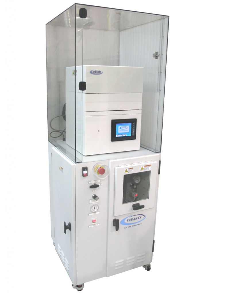
The PRIMAXX® Vapor HF Etching System is a precision dry etching tool designed for isotropic removal of silicon dioxide using vapor-phase hydrofluoric acid. Its anhydrous process eliminates stiction, making it ideal for delicate microstructures. Widely applied in MEMS fabrication, nanotechnology, and semiconductor research.
Capable of processing wafers up to 200 mm (8 inch)
Specification/resolution
Etch method: Vapour-phase hydrofluoric acid (HF) Etch rate: controllable, typically 60~100 nm/min Stiction-free release process for suspended structures Compatible with MEMS and nanodevices requiring critical dimension control
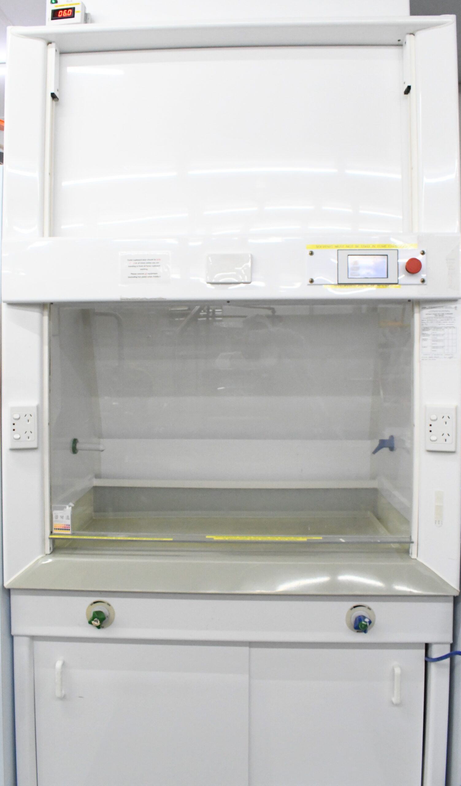
Wet etching is a chemical process used to selectively remove materials from a substrate by immersing it in a liquid etchant. It is commonly used in microfabrication and materials research to define patterns or clean surfaces with controlled precision inside a a fume cupboard (or fume hood) is a ventilated enclosure that provides a safe workspace for handling hazardous chemicals. It protects users by drawing away fumes, vapors, and particles, ensuring safe execution of processes such as wet etching.
Example of use
Wet chemical etching of metals and oxides Surface preparation and cleaning of semiconductor substrates Sample cleaning
Purpose:
Used for a variety of wet-chemical processes required in microfabrication and device preparation.
Available wet processes
Aluminium and nickel etching Buffered HF (BHF) and HF-related processes Keller’s’ reagent etching RCA cleaning Piranha cleaning KOH etching
Scale/volume:
Capable of handling fragments to full wafers (up to 6-inch).