Lithography
Our Lithography Capabilities Support Three Key Areas:
- Standard Lithography Suite
- Microfluidics Platform and Soft Lithography
- Nano 3D Printing
SUSS MicroTec MA/BA6 Gen4 Mask Aligner
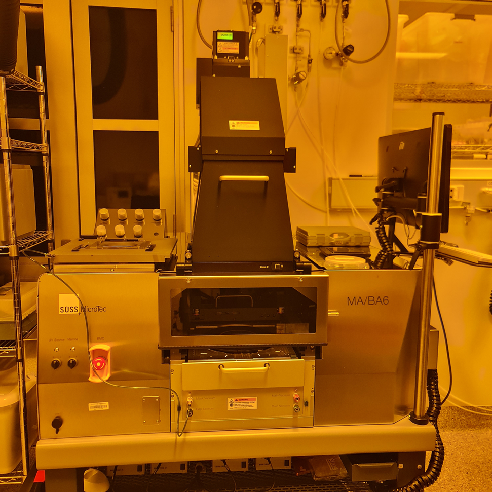
The SUSS MicroTec MA/BA6 Gen4 is a specialized semi-automated mask aligner designed for high-precision photolithography applications in research and prototyping. It supports flexible exposure modes and multiple alignment technologies, making it highly suitable for fabricating microdevices, MEMS, microfluidic chips, and photonic structures at ANFF-Qld.
PurposeThe MA/BA6 Gen4 transfers photomask patterns onto photoresist-coated substrates with precise overlay control. It supports top-side, bottom-side, and infrared (IR) alignment, allowing for complex multilayer wafer processing and backside alignment. The system efficiently processes wafers from 2” up to 6” diameter.
Examples of Use
- MEMS and NEMS fabrication
- Microfluidics device prototyping
- Semiconductor and compound semiconductor research
- Photonics and optoelectronics
- Sensor and advanced material microfabrication
Key Features
- Alignment Accuracy: Sub-micron precision, achieving approximately ±0.5 µm for top-side alignment and ±1 µm for backside alignment
- IR Illumination: Infrared alignment capability for backside alignment and multilayer wafer fabrication on IR-transparent materials such as GaAs, InP, and silicon
- Wafer Sizes: Supports wafers from 2” (50 mm) to 6” (150 mm) in diameter with substrate thickness up to 10 mm
- UV Illumination: Energy-efficient UV LED illumination system covering G-, H-, and I-lines (350–450 nm) for compatibility with a wide variety of photoresists
- Auto Alignment: High-precision automated alignment utilizing advanced digital microscopes and cameras for accurate target recognition and placement
- Thick Film Compatibility: Supports processing of thick photoresists including SU-8 and dry film resists for MEMS and microfluidic applications
- Exposure Modes: Soft, hard, vacuum contact, and proximity (adjustable gap down to 1 µm)
- Optical System: Includes high-resolution digital microscopes
- Ergonomic Design: Designed to maximize throughput and user comfort with intuitive software, recipe management, and safety features
Model: SUSS MicroTec MA/BA6 Gen4
Site: The University of Queensland
Location: Class 1000 cleanroom, Level 2E, AIBN (Bldg #75), St Lucia
Instrument Contact: Dr Shuvashis Dey
Maskless Aligner – MLA150
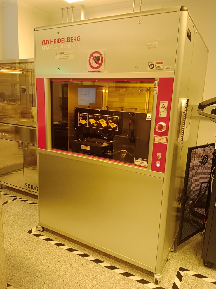
The Heidelberg MLA150 is a high-speed, maskless direct-write photolithography system designed for research, prototyping, and semiconductor fabrication. Unlike traditional systems, it eliminates the need for costly photomasks by directly exposing patterns onto wafers with a laser. This approach reduces costs, enables rapid design changes, and significantly shortens turnaround time from concept to prototype.
Purpose
The MLA150 transfers patterns directly from CAD files onto photoresist-coated substrates. With flexible frontside and backside alignment and support for multilayer structures, it is ideal for advanced prototyping and research applications that demand high accuracy and speed.
Examples of Use
- MEMS and microfluidics
- Micro-optics and photonic structures
- Semiconductor research and prototyping
- Sensor development
- Mask fabrication
- Advanced materials and device research
Resolution and Specification
- Minimum feature size: ~1 µm (depending on resist and process conditions)
- Laser wavelengths: 375 nm and 405 nm for compatibility with a wide range of photoresists
- Frontside and backside alignment with high overlay accuracy
- Direct writing from CAD files for streamlined design-to-prototype workflows
Model: MLA 150
Site: The University of Queensland
Location: Class 1000 cleanroom, Level 2E, AIBN (Bldg #75), St Lucia
Instrument Contact: Dr Jaber Saghaei

Direct Write Laser System for Chrome Mask Production
The Heidelberg µPG101 is a direct write laser system used to write photolithography chrome masks. The system has a maximum write resolution of 2 µm and a maximum write area of 125 mm x 150 mm. The system can write to 5” and 7” chrome masks.
ANFF-Q will write designs on request, develop, etch, clean, inspect and ship masks to your location.
Examples of use:
The system can be used for applications such as MEMS, bio MEMS, integrated optics, microfluidics, sensors, actuators, MOEMS, material research, nanotubes, graphene, and any other application that requires high precision, high-resolution microstructures.
- Purpose: Direct laser writer for creating high resolution 2D patterns on chrome masks.
- Material systems: UV curable polymers on chrome coated soda lime substrates.
- Scale/volume: Writes to 5” and 7” masks.
Specifications/resolution:
- Mode 1: Write area 90 mm x 90 mm with a resolution of 2 µm
- Mode 2: Write area 125 mm x 150 mm with a resolution of 5 µm
- Model: Heidelberg µPG101
- Site: The University of Queensland
- Location: Class 1 000 cleanroom, Level 2E, AIBN (Bldg #75), St Lucia
- Instrument Contact: Jane Li
Hexamethy ldisilizane (HMDS) Oven
The Hexamethyldisilazane (HMDS) Oven is used to enhance photoresist adhesion on silicon and glass substrates. Before spin coating, the substrate surface is primed through vapour-phase deposition of HMDS, creating a hydrophobic surface that improves resist bonding. This process begins with a dehydration bake at 150 °C to remove residual moisture, ensuring a stable and clean surface for priming.
Purpose
The HMDS oven is essential for reliable photolithography, particularly when fabricating small or high aspect ratio features where strong adhesion is critical. By improving resist-substrate bonding, it reduces resist lift-off and pattern failure during development and subsequent processing.
Examples of Use
- Standard photolithography processes
- Fabrication of high-resolution or high aspect ratio microstructures
- MEMS and semiconductor device processing
- Optical and microfluidic device prototyping
Specifications
- Priming method: Vapour-phase HMDS deposition
- Pre-treatment: Dehydration bake at 150 °C
- Substrates: Compatible with silicon, glass, and similar surfaces
- Limitation: Not effective with SU-8 photoresist (Ti Prime recommended instead)
Model: YES LP-III Oven
Site: The University of Queensland
Location: Class 10000 cleanroom, Level 2E, AIBN (Bldg #75), St Lucia
Instrument Contact: Dr Jaber Saghaei
 Hot Embosser
Hot embossing is a micro replication process that replicates a microstructured master, sometimes referred as a mould insert or a stamp, in polymer. The embossing process involves pressing the stamp onto a material, usually thermal plastic, and heating up the material to its glass transition temperature while applying hydraulic pressure. This process replicates the microstructures on the material, which is then allowed to cool and removed from the stamp.
The EVG520IS semi-automated single-chamber hot embossing unit handles wafers up to 150 mm with semi-automated operation for small volume production applications. The equipment is custom designed to have maximum temperature of 650 °C and pressure up to 60 kN.
The EVG520IS features EV Group’s proprietary symmetric rapid heating and a cooling chuck design. The key advantages of the EVG hot embosser are an independent top and bottom side heater, a high pressure bonding capability and same material and process flexibility. The EVG520IS is also equipped with anodic bonding facility for packaging glass and silicon wafers. This additional feature is capable of monitoring bonding continuously displaying bond parameters with a high resolution display of the bond current down to 20 μA resolution and a high voltage power supply of 2 000 V/50 mA. The bond parameters, including current, can be adjusted using a software interface.
Examples of use:
The EVG520IS system can be used in hot embossing of thermal plastics, nanoimprint lithography, and wafer to wafer bonding for MEMS and packaging devices.
Purpose:
Stamping of a pattern into a polymer substrate softened by raising the temperature just above its glass transition temperature primarily for defining micro channels and wells for fluidic devices. A wide variety of polymers can be used to hot emboss.
Bonding of wafers, such as fusion bonding (silicon to silicon), anodic bonding (Pyrex to silicon), eutectic bonding (Si to Si with metal), and adhesive assisted bonding.
Material systems:
Polymers with glass transition temperature below 650 °C, silicon, pyrex wafers.
Scale/volume:
- Stamp size and substrate size up to 150 mm (6 inch).
- One sample at a time.
- Minimum wafer diameter: 80 mm.
- Fully-automated single chamber processing with manual loading and unloading including external cooling station.
Specifications/resolution:
- Semi-automated system with temperatures of up to 650 °C and 60 kN pressure.
- Rapid substrate cooling.
- Fully automated bond process execution and bond cover movements with multi-stack bonding option.
- Integrated top and bottom side cooling station for high throughput.
- Bond chuck system/alignment system: 100 mm and 150 mm wafer using EVG620
- Maximum contact force: up to 60 kN
- Maximum temperature: 650°C
- Vacuum: 10 – 3 mbar
- Power supply for anodic bonding: 0 – 2.000 V/50 mA
Model: EVG520IS
- Site: The University of Queensland
- Location: Class 1 000 cleanroom, Level 2E, AIBN (Bldg #75), St Lucia
- Instrument Contact: Jaber Saghaei
 Lithography Suite
The lithography suite at ANFF-Q’s Griffith University site is set for processing micron features using positive and reverse image photoresist.
All processes are recipe driven ensuring consistent quality processing for full wafers. Typical resist thickness uniformity for 150 mm wafer = <+/- 0.5 %. Sub-micron lithography capability has been shown.
The lithography suite of equipment provides the complete process flow for industrial standard processing, i.e. priming, coating, softbake, exposing, developing and hardbake.
Although the suite is set for 150 mm, processing smaller wafers and fragment processing is also possible.
For more detailed specifications and capabilities of the lithography equipment see pdf files at Queensland Microtechnology Facility and Queensland Micro- and Nanotechnology Centre.
- Purpose: Commercial standard photoresist patterning for device fabrication.
- Material systems: Si wafers.
- Scale/volume: 150 mm manual handling and wafer fragments.
- Specifications/resolution:
Recipe driven processing ensuring consistent quality resist 1 µm thick coating, non uniformity < +/- 0.5 % with 3 mm edge exclusion, achieved resolution: 1 µm lines and spaces with 86 ° profile on targeted features.
Site: Griffith University
Location: Cleanroom, QMF, N74 (Bldg N74), Nathan Campus
Instrument Contact: Pradip Singha

Microfluidics Platform
Microfluidics is an emerging technology that operates in the micrometre scale, which has been widely used in biology, chemistry and biotechnology experiments for multiplexing, automation and high throughput screening due to its advantages such as low sample requirements, high surface area and reduced system footprint. ANFF-Q has a fully equipped microfluidics platform including an inverted fluorescence microscope, high speed camera and syringe pumps, which provides users a multifunctional platform to perform most microfluidic experiments.
Examples of use
The ANFF-Q microfluidics platform equipped with two dual drive syringe pumps and a Phantom high speed camera can be used to generate picolitre droplets in microchannels, a technique which has been widely used in several interesting applications such as drug delivery, cell encapsulation, RNA-Seq and bioreactors. Combined with the fluorescence microscope, this platform enables users to analyse the fluid diffusion, chemical reactions and cell activities based on the fluorescent markers.
Purpose:
Providing a one-stop platform for performing microfluidic experiments.
Related Equipment:
Nikon Ti Inverted microscope with motorized stage.
Two Harvard Apparatus Dual Drive System pumps.
SPECTRA X Light Engine with full wavelength filters.
Nikon camera comes with NIS-Elements Imaging software.
Phantom VEO E-340L high speed camera with a frame rate of up to 287,000.
Site:
The University of Queensland
Location: PC2 Lab, Level 2E, AIBN (Bldg #75), St Lucia
Instrument Contact: Dr Shuvashis Dey
Nano 3D Printing
ANFF-Qld provides world-class nano-3D printing capabilities through its two Nanoscribe systems. The Photonic Professional GT is a two-photon lithography platform, ideal for fabricating highly precise micro- and nano-scale 3D structures. Complementing this, the MPO 100 is a cutting-edge multi-photon lithography system, offering advanced functionality and greater versatility for complex designs and applications in photonics, micro-optics, and biomedical engineering.
Nanoscribe 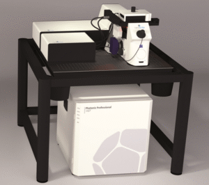
The Nanoscribe Photonic Professional GT is an advanced 2 photon 3D lithography system that allows structures to be printed with a building block as small as 100 nm in size. A wide range of photoresists can be written to, in addition to a number of substrates ranging from coverslips to 5” square masks. The precision stage control allows intricate structures such as photonic crystals or meta-materials to be easily fabricated. In addition, larger structures can be written such as microfluidic channels allowing novel channel shapes to be easily constructed.
Examples of use:
- Photonic crystals
- 3D projections
- Microfluidics
- Cell scaffolds
- Bio mimicry
- Material systems:
- Polymers
- Scale/volume:
Range of substrates from cover slips and microscope slides up to 4” silicon wafer and 5” square.
Specifications: Structures can be built with a minimum voxel size of 100 nm x 350 nm.
Model: Nanoscribe Photonic Professional GT
Site: The University of Queensland
Location: Class 10,000 cleanroom, Level 2E, AIBN (Bldg #75), St Lucia
Instrument Contact: Dr Jane Li
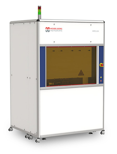
MPO100
The MPO 100 is a high-end multi-photon 3D printer designed for rapid prototyping and advanced microfabrication. It combines the resolution of two-photon polymerization with the scalability of microfabrication, making it possible to produce structures from the nano to millimetre scale with submicron precision. The system is optimized for both scientific research and industrial applications, supporting a wide range of photoresists and substrates. Its high-precision laser scanning and stage control enable complex 3D structures, functional micro-optics, and biomedical scaffolds to be fabricated with speed and reliability.
Examples of use:
• Micro-optics and diffractive optical elements
• Microlenses and freeform optics
• Micro-mechanical parts
• Biomedical scaffolds
• Microfluidic components
Material systems:
Polymers
Scale/volume:
From nanostructures on coverslips and slides up to centimetre scale parts on 4” wafers.
Specifications:
Structures can be built with submicron resolution (minimum feature size ~100 nm).
Model: MPO 100
• Site: The University of Queensland
• Location: Class 10,000 cleanroom, Level 2E, AIBN (Bldg #75), St Lucia
• Instrument Contact: Dr Jane Li
 Oxygen Plasma Cleaner
Plasma cleaning involves the removal of impurities and contaminants from surfaces through the use of an energetic plasma or dielectric barrier discharge plasma created from gaseous species. ANFF-Q’s oxygen plasma cleaner can be employed for plasma surface cleaning and surface treatment for various application fields, including materials science, polymer science, biomedical materials, microfluidics, optics, microscopy, and dental and medical research.
Examples of use:
Surface cleaning, sterilisation, activation, energy alteration, and preparation for bonding and adhesion (such as PDMS device fabrication); surface treatment of polymers and biomaterials through activation, grafting and surface coating; modification of surface chemistry—e.g. contact angle measurements on plasma-treated glass and polymer materials show enhanced surface wettability.
Purpose:
Nanoscale surface cleaning and surface activation.
Material systems:
Silicon, glass, PDMS, etc.
Scale/volume:
Up to 4 inch substrate.
Specifications/resolution:
Oxygen plasma, power 10 – 30 W.
Model:
Harrick Plasma expanded plasma cleaner (PDC-001 and PDC-002)
- Site: The University of Queensland
- Location: PC2 Laboratory, Level 2E, AIBN (Bldg #75), St Lucia
- Instrument Contact: Dr Shuvashis Dey
 Tergeo Plasma Cleaner
Plasma cleaning involves the removal of impurities and contaminants from a surface through the use of an energetic plasma generated from gaseous species. There are two gases — oxygen and nitrogen — available for the ANFF-Q’s Tergeo plasma cleaner, which can be employed to remove hydrocarbon and other types of surface organic coatings or contaminations, change surface energy and improve the bonding strength. The Tergeo plasma cleaner comes with a 4” diameter X 6.5” length Pyrex chamber and is able to generate adjustable RF power up to 75W.
Examples of use:
PDMS, microfluidics, glass slides and lab-on-a-chip. Improve bonding for plastic, polymer and composite materials. Device activation, sterilization and surface cleaning for organic contamination removal.
Purpose:
Surface activation and cleaning.
Material systems:
PDMS, glass, silicon, plastic and metal.
Scale/volume:
Up to 4 inch substrate.
Specifications/resolution:
Oxygen and nitrogen plasma with an adjustable power up to 75W.
Model:
Tergeo Tabletop Plasma Cleaner
Site:
The University of Queensland
Location:
Class 10 000 cleanroom, Level 3, Pandanus (Bldg #1022), Long Pocket
Instrument Contact: Dr Shuvashis Dey
Photolithography
Photolithography allows patterning of substrates for a wide range of applications such as MEMs, optics and microfluidics. Our photolithography workflows consist of a collection of tools including spin coaters, hotplates, mask aligners and fume cupboards for photoresist development. All glassware is provided and photoresists can be ordered through the facility. There are four separate streams for photolithography processes in the ANFF-Q cleanroom, as detailed below.
 AZ stream
This stream allows users to pattern substrates using AZ series photoresists.
Examples of use:
Patterning of metal lift-off, dry etch masking, wet etch masking.
Material systems:
AZ12XT and AZ nLOF 2020 are dispensed automatically. Other AZ series photoresist (AZ40XT, AZ 1518 and AZ 1505) are allowed. Consult staff before use.
Scale/volume:
4” and 6” round wafers; consult staff for substrates of other sizes.
Specifications/resolution:
Spin coater (Sawatec SM-200): up to 6000 rpm with edge bead removal and backside rinse, with automatic resist dispensing.
Hotplate (Sawatec HP-200): up to 250 °C with lift pins and a glass cover. HMDS vapour priming available in the same chamber.
Mask Aligner (EVG620): front side and backside alignment.
Site:
The University of Queensland
Location:
Class 10 000 cleanroom and class 1 000 cleanroom, Level 2E, AIBN (Bldg #75), St Lucia
Instrument Contact:
 SU8 Stream
This stream allows users to pattern substrates using SU8 series photoresists.
- Examples of use: SU8 microfluidic moulds for soft lithography processes.
- Material systems: SU8 polymers, commonly SU8 2000 and SU8 3000 series.
- Scale/volume: 4” and 6” round wafers; consult staff for substrates of other sizes
Specifications/resolution:
- Spin coater (SPS Polos SPIN 150i): up to 12 000 rpm, no edge bead removal available.
- Hotplate with aluminium top (Torrey Pines HP51A): up to 450 °C. Stirring function available.
- Mask Aligner (EVG620): front and backside alignment.
- Site: The University of Queensland
- Location: Class 10 000 cleanroom and Class 1 000 cleanroom, Level 2E, AIBN (Bldg #75), St Lucia
- Instrument Contact: Dr Shuvashis Dey
 Dry Film Stream
This stream allows users to pattern substrates using dry film epoxy.
- Examples of use: SU8 microfluidic moulds for soft lithography processes.
- Material systems:ADEX and SUEX dry films of varying thicknesses by DJ Microlaminates.
- Scale/volume: 4” and 6” round wafers; consult staff for substrates of other sizes.
Specifications/resolution:
- Dry film laminator (Sky 335R6): Laminator with roller speed up to 1.35 m/min and temperature up to 140 °C.
- Digital programmable hotplates (Torrey Pines HP40A): up to 450 °C. Stirring function available. Programmed for slow temperature ramping.
- Mask Aligner (EVG620): front and backside alignment.
- Site: The University of Queensland
- Location: Class 10 000 cleanroom and class 1 000 cleanroom, Level 2E, AIBN (Bldg #75), St Lucia
- Instrument Contact: Dr Shuvashis Dey
 Novel Stream
This stream allows users to pattern substrates using other polymer or resist systems containing photoinitiator.
- Examples of use: Polymer coating.
- Material systems: User defined. Consult staff before use.
- Scale/volume: Small scale square substrates only.
Specifications/resolution:
- Spin coater (Osilla): up to 6000 rpm with vacuum-free chucks.
- Hotplate with aluminium top (Torrey Pines HP51A): up to 450 °C. Stirring function available.
- Mask Aligner (EVG620): front and backside alignment.
- Site: The University of Queensland
- Location: Class 10 000 cleanroom and class 1 000 cleanroom, Level 2E, AIBN (Bldg #75), St Lucia
- Instrument Contact: Jane Li
Silanisation Dessicators
Treatment of surfaces to change how fluids interact with them is a critical step in constructing useful microfluidics devices, especially those used in biological applications. Silanisation is the generic term applied to the formation of organosilane monolayers on substrates. These monolayers can be subsequently modified to produce a surface with a specific functionality.
ANFF-Q has two dedicated silanisation bell jar dessicators from ProSciTech, allowing the silanisation process to be performed simply and easily.
Examples of use:
- Silanisation increases hydrophobicity and can be used in cell culturing to reduce adherence of cells to flask walls.
- Silanising the surface of a mould (PDMS Master) is important to prevent PDMS adhering to the master, which would make it more difficult to release the mould and potentially damage the master.
Purpose:
Modification of substrates for microfluidic purposes, PDMS device fabrication and surface modification for biological application of microfluidic devices.
- Material systems: Organic, inorganic and biological.
- Site: The University of Queensland
- Location: PC2 Lab, Level 2E, AIBN (Bldg #75), St LuciaClass 10 000 cleanroom, Level 3, Pandanus Building (#1022), Long Pocket
- Instrument Contact: Wael Al Abdulla
 Soft Lithography
Soft lithography provides access to three-dimensional and curved structures, tolerates a wide variety of materials, generates well-defined and controllable surface chemistries, and is generally compatible with biological applications. PDMS is a low cost, chemically inert, and biocompatible material, with a versatile surface chemistry and flexible mechanical properties that has been widely used in soft lithography for various applications, including microfluidics, lab-on-a-chip and cell biology.
ANFF-Q has a fully equipped soft lithography suite at the UQ Long Pocket campus. The soft lithography suite is located within a class 10 000 cleanroom, allowing our clients to fabricate advanced microfluidic devices from start to finish within a dedicated clean environment, ensuring the entire process is dust free.
Examples of use
Soft lithography can be used for microfluidics device fabrication, bonding and micromoulding.
Related equipment:
- Planetary mixer for PDMS mixing and degassing.
- Spin coater for PDMS coating on wafer and glass slides.
- Silanisation desiccators for surface treatment.
- Ovens and hotplates for curing.
- Ultrasonic cleaner for glass slides cleaning.
- Tergeo plasma cleaner for surface activation and device bonding.
- Zeiss optical microscope for device examination.
Purpose:
PDMS device fabrication and surface modification for biological applications.
- Material systems: Organic, inorganic and biological.
- Site:The University of Queensland
- Location: Class 10 000 cleanroom, Level 3, Pandanus Building (#1022), Long Pocket
- Instrument Contact: Dr Shuvashis Dey
 Spin Coaters
Spin coating is a technique used to apply uniform thin films to flat substrates. A sample diluted in a moderate boiling point material is applied to a substrate that is undergoing rotation.
Spin coaters can be used to apply thin polymeric films to silicon wafers in the development of soft-resists in the photolithography process. The thickness of films that are applied can be less than 10 nm and are governed by the concentration of the polymeric solution applied and the rotation speed.
ANFF-Q has a Brewer Science spin coater for SU8 and an APT Polos spin coater for PDMS that take various wafer geometries from 10 mm to 6” in diameter.
Purpose: For spin coating of photoresist and polymers on glass and silicon wafer and other substrates.
Material systems: Positive and negative photoresist and other polymers.
Scale/volume: Wafer size up to 150 mm (6 inches).
Specifications/resolution:Chemical resistant spin bowl and body, manual operation, closing lid and is fully programmable with alignment wafer tool.
Model:
Brewer Science CEE 200X spin coater
- Site: The University of Queensland
- Location: Class 10 000 cleanroom, Level 3, Pandanus Building (#1022), Long Pocket
- Instrument Contact: Dr Shuvashis Dey
Planetary mixer
The Planetary mixer at ANFF-Qld is designed for mixing and degassing PDMS (Polydimethylsiloxane) mixtures used in soft lithography. This mixer ensures homogenous mixing while removing air bubbles efficiently to optimize PDMS quality for microfabrication applications.
Purpose
The mixer combines planetary and revolution movements to thoroughly mix PDMS and degas simultaneously. It is suitable for small batch preparation to sustain high reproducibility in resist processing for advanced device fabrication.
Equipment Details
- Name: Planetary Mixer
- Manufacturer: Kurabo
- Model: KK-V300SS
Location: Class 10 000 cleanroom, Level 3, Pandanus Building (#1022), Long Pocket
Instrument contact : Shuvashis Dey
 UV–Ozone cleaner
The MBRAUN MB-UV-O3 cleaner is an integrated system for UV ozone cleaning of semiconductor and optical surfaces. This process provides a clean, hydrocarbon-free optical surface with significantly improved thin film and UV resin adhesion characteristics.
Applying ozone and UV light simultaneously, results in a highly effective removal of residual organic and carbon contamination down to contact angles of 5 degrees (depending on initial cleaning and substrate material).
ANFF-Q’s UV–ozone cleaner is housed within our encapsulation glove box.
Examples of use
The UV–ozone cleaner has a number of applications, including:
- Surface cleaning
- Preparation of surfaces for thin film deposition and surface treatment
- UV curing
- Surface sterilization
- Improving surface hydrophilicity
- Removal of surface monolayers
Purpose:
Preparation of surfaces.
Material systems:
Organics, metals and dielectrics.
Scale/volume:
Substrate size up to 150 mm x 150 mm.
Specifications/resolution:
The control unit allows you to set the process (irradiation) time from 1 to 999.9 minutes while an integrated flow meter is used to adjust the process gas flow during the cleaning process. Once the pre-set irradiation time has ended, the oxygen flow is automatically shut off and the process chamber is purged with nitrogen until all process gases have been removed. Integrated safety interlocks are provided to shut off the UV radiation if the door is opened during the process or if the exhaust is interrupted.
Wavelength: main peaks at 184.9 nm and 253.7 nm.
Model:
Site:
The University of Queensland
Location:
Room 910, Level 9, COPE (Bldg #68), St Lucia
Instrument Contact:
3D printing suite
3D printing is used in research, rapid prototyping and additive manufacturing. 3D printing builds a three-dimensional object from a computer-aided design (CAD) model. 3D printers can create objects of almost any shape or geometry usually by successively adding material layer by layer. There are many different technologies used to achieve this, including low force stereolithography (LFS), fused filament fabrication (FFF) and Digital Light Processing (DLP).
At ANFF-Q, we are moving to nano scale researchand we only keep Ultimaker 2 Extended+ 3D printer:
Ultimaker 2 Extended+ 3D printerv

The Ultimaker 2 Extended+ is a desktop fused filament fabrication (FFF) 3D printer. The Ultimaker 2 Extended+ uses an open filament system so you are able to use any kind of filament you want to achieve precisely the finish you’re after. And due to the interchangeable nozzles, you can go from 800 µm all the way down to a finely detailed 150 µm in lateral resolution with a layer thickness between 20 µm and 600 µm. This gives you the freedom to create really fast drafts, detailed prints and everything in between.
Examples of use
The Ultimaker 2 Extended+ can be used in prototyping and part design as well as to create niche items for immediate use. Uses range from biomedical applications through to parts manufacture and jewellery.
Purpose: To create complicated 3D structures.
Material systems:
Open filament system; optimised for PLA, ABS, CPE, CPE+, PC, Nylon and TPU 95A.
Scale/volume:
Build volume: 223 × 223 × 305 mm
Specifications/resolution: Layer thickness: 20 – 600 µm
Lateral resolution: 150 um to 800 um
Build speed: up to 24 mm3/s
Travel speed: up to 300 mm/s


