Deposition
Electron beam evaporation system

The Temescal FC-2000 e-beam evaporator is a fast- cycle, load-locked electron beam evaporation system that allows the source to remain under vacuum during substrate reloading. There are six source pockets in the chamber which allows for multiple layer coating without breaking vacuum.
Currently the available evaporation materials are: Al, Ni, Cr, Ag, Au, Ti, Cu, NiO, TiO2, MoO3, Al2O3 and ITO.
Examples of use: Device metallisation, metal interconnection, solar cells.
Purpose: To coat a uniform metal layer and dielectrics film.
Material systems: Inorganic compounds and metals.
Scale/volume: Up to 13 pieces of 4 inch wafer.
Specifications/resolution: Deposition rate 1 – 2 Å/s, up to 300 degrees Celsius substrate heater with 2 reactive gases, 6 crucible pockets.
E-gun power: 10 KV
Model: Temescal FC-2000 E-Beam Evaporator
Site: The University of Queensland
Location: Class 10 000 cleanroom, Level 2E, AIBN (Bldg #75), St Lucia
Instrument Contact: Kai-Yu Liu
Electron beam evaporation system HHV ATS500
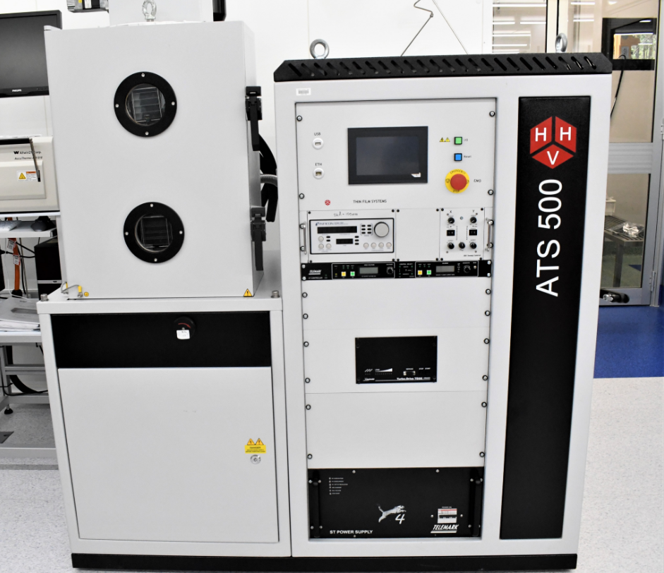
The HHV ATS 500 e-Beam Evaporator is a versatile thin-film deposition system designed for advanced research and small-scale production. Its high-vacuum capability, and customisable substrate handling ensure precision, repeatability. Ideal for semiconductor, optical, and nanotechnology applications.
Examples of use: Device metallisation, metal interconnection, solar cells.
Purpose: To coat a uniform metal layer and dielectrics film.
Material systems: Metals and semiconductor compounds (about 15 types of materials available)
Scale/volume: Up to 4 pieces of 6 inch wafers in a single deposition.
Specifications/resolution: Deposition rate 1 – 3 Å/s, up to 200 degrees Celsius substrate heater with reactive oxygen gas, 4 cruicble pockets.
E-gun power: 6 KV
Model: ATS500 Evaporator
Site: Griffith Uiversity
Location: Cleanroom, QMF, N74 (Bldg N74), Nathan Campus
Instrument Contact: Nhat Khuong Nguyen
Oxidation furnace

The HiTech benchtop oxidation furnace is a very user-friendly system with an auto loading/unloading feature. It can be used for wet/dry oxidation and annealing process.
Examples of use: Silicon dioxide growth.
Purpose: Used to grow oxide layers on silicon wafers at temperature up to 1 100 degrees Celsius.
Material systems: Silicon only.
Scale/volume: Multi wafers to a maximum of 25.
Specifications/resolution: Max temperature: 1 200 degrees C.
Model: HiTech benchtop oxidation furnace
Site: The University of Queensland
Location: Class 10 000 cleanroom, Level 3, Pandanus (Bldg #1022), Long Pocket
Instrument Contact: Kai-Yu Liu
Dry Oxidation Furnace
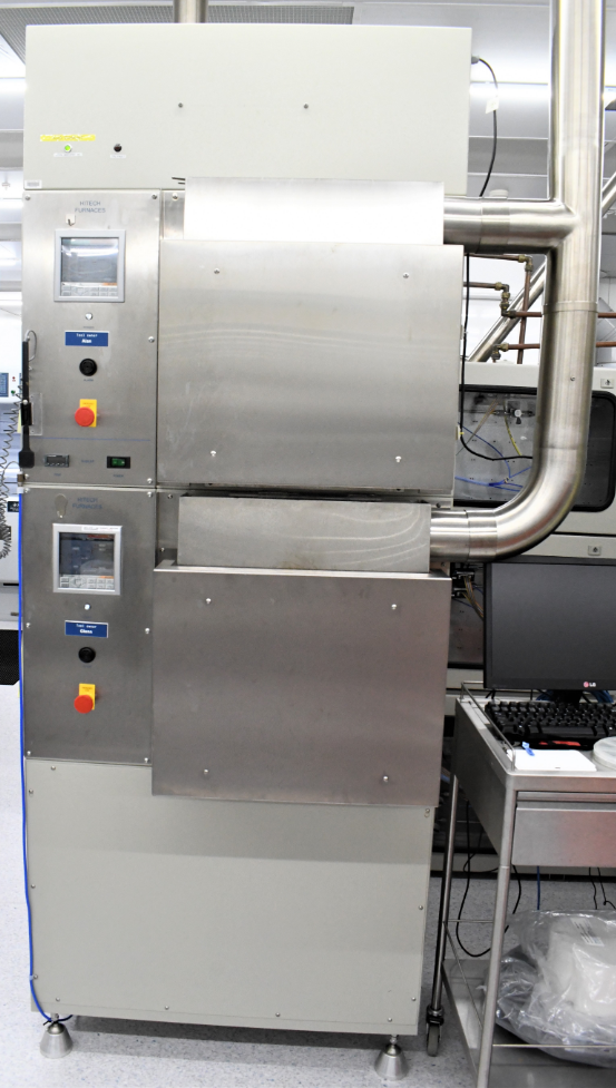
The HiTech oxidation furnace is specialised for dry oxidation processes, capable of oxidising both silicon (Si) and silicon carbide (SiC) into thermal oxide thin film using oxygen (O₂) and nitric oxide (NO) gases.
Examples of use
Thermal oxide growth on Si and SiC substrates
Purpose
Used to grow high-quality thermal oxide layers on silicon and silicon carbide at elevated temperatures.
Material Systems
Silicon (Si) and silicon carbide (SiC).
Scale/Volume
Fragments and wafers up to 6-inch diameter
Specifications/Resolution
Max temperature: 1200 °C
Dry oxidation only with reactive oxygen and nitric oxide gases
Uniform processing across full wafer load
Model
HiTech dry Oxidation furnace
Site
Griffith University
Location
Cleanroom, QMF, N74 (Bldg N74), Nathan Campus
Instrument contact
LPCVD furnace, HiTech
The HiTech LPCVD furnace is a furnace reactor designed for uniform thin-film deposition of silicon dioxide using silane (SiH₄) and oxygen (O₂) vacuum conditions.
Examples of use
Silicon dioxide deposition from SiH₄ and O₂.
Purpose
Used to deposit high-quality SiO₂ films on silicon wafers at elevated temperatures.
Material Systems
Deposition of SiO₂ films.
Scale/Volume
Maximum of 10 of 6-inch wafers or single 8-inch wafer
Specifications/Resolution
Deposition temperature: 600°C
Uniformity across full wafer load
Model
HiTech LPCVD Furnace
Site
Griffith University
Location
Cleanroom, QMF, N74 (Bldg N74), Nathan Campus
Instrument contact
SiC deposition on Si wafers
At ANFF-Q, we would like to promote the use of SiC technology. ANFF-Q has two SiC deposition systems available within the Queensland Microtechnology Facility to supply SiC coatings on Si substrates.
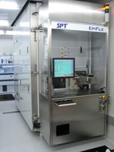
The EpiFlx reactor
Created in partnership with SPT Microtechnologies USA, a large production batch reactor for up to 300 mm wafers.
Various epitaxial deposition processes are available for 3C SiC deposition on Si <100> and <111> and also on epitaxially grown AlN. SiC can also be deposited on silicon oxide and silicon nitride films on Si wafers.
We actively seek to promote the use of the silicon carbide on silicon (SiC on Si). If you are interested in research collaboration or product development in SiC on Si applications, please contact the ANFF-Q Facility Manager.
For more detailed specifications and capabilities see information and pdf files at Queensland Microtechnology Facility.
Examples of use:
Because there is a large variety of 3C SiC with different attributes possible, we like to discuss the application needs of each client in order to select and qualify the deposition process to provide the best and most suitable material for each application.
Purpose:
- Provide a production ready process solution to exploit the superior properties of SiC for use in the next generation of devices:
- MEMs
- NEMs
- Optical
- Photonics
- Diaphragms
- Filters
- Bio sensors
- Si substrates targeting applications such as GaN substrate or HEMT and LED
- SiC on Si substrate for graphene
Material systems:
Standard Si wafers.
Scale/volume:
Small samples to large batch processes for up to 300 mm wafers.
Specifications/resolution:
Typically SiC film thicknesses available from 20 nm to 1 µm with thickness non uniformity <1 %, 1 mm edge exclusion.
SiC on Si with a sub nm rms surface roughness is available.
Site
Griffith University
Location:
QMF (Bldg N74), Nathan Campus
Instrument Contact:
Inductively Coupled Plasma CVD, Oxford Instruments PlasmaPro 100
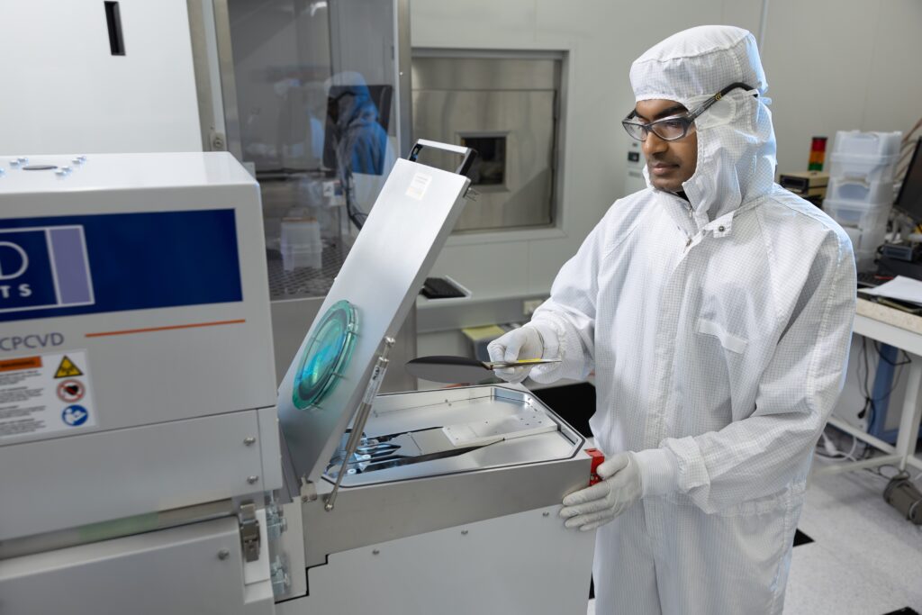
The Oxford Inductively Coupled Plasma Chemical Vapor Deposition (ICPCVD) system is designed for high-quality thin-film growth with excellent step coverage, density, and uniformity. Its low-temperature plasma-enhanced process ensures compatibility with temperature-sensitive substrates while maintaining precise film control. Ideal for semiconductor, MEMS, photonics, and nanotechnology applications.
Examples of use
Dielectric passivation (SiO₂, SiNₓ)
Gate dielectrics
Optical coatings
MEMS protective layers
Purpose
To deposit uniform dielectric and semiconductor films with high conformality and controlled stoichiometry.
Material Systems
Silicon dioxide (SiO₂)
Silicon nitride (SiNₓ)
Amorphous silicon (a-Si:H)
Silicon carbide (SiC)
Other dielectric films (on request)
Scale/Volume
Up to 6-inch wafers
Specifications/Resolution
Deposition rate: ~10–20 nm/min (process-dependent)
Substrate temperature: 100 – 200 °C (typical)
RF Inductively Coupled Plasma source with independent RF bias
Excellent film uniformity across 6-inch wafers (<±5%)
Compatible with O₂, N₂, NH₃, SiH₄, and other reactive gases
Model
Oxford Instruments PlasmaPro 100 ICPCVD
Site
Griffith University
Location
Cleanroom, QMF, N74 (Bldg N74), Nathan Campus
Instrument contact
Sputtering system

The AJA ATC 2200 sputtering system has two RF and two DC power generators which can cater for various material depositions. It is equipped with a vacuum load-lock which gives two major advantages of higher throughput and better film quality.
Argon, nitrogen and oxygen are available for use in reactive ion sputtering applications. The reactive gas chemically combines with the target material to form a different material on the substrate. The substrate holder can be heated up to 350 degrees Celsius for a higher sputtering rate and the system is also capable of applying RF-bias to do sample sputtering clean before deposition.
The substrate holder is designed for an 8 inch wafer, but it can also be adjusted to hold 4–6 inch wafers. The substrate holder can be rotated during deposition to improve film uniformity.
Examples of use:
Film coating for solar cells.
Purpose:
The plasma enhanced deposition technique is used to generate a variety of materials at the atomic scale. Novel materials and structures are formed in the presence of the reactive gases.
Material systems:
Inorganic target compounds, dielectric materials and metals.
Scale/volume:
Single wafer processing up to 8 inches.
Specifications/resolution:
Reactive gases: N2, O2, Ar; 4 Targets: 2 RF and 2 DC; a loadlock robotic system; plasma cleaning and a base vacuum of 10 – 8 Torr.
Model:
Site:
The University of Queensland
Location:
Class 10 000 cleanroom, Level 2E, AIBN (Bldg #75), St Lucia
Instrument Contact:
Magnetron sputterer, SNS gamma
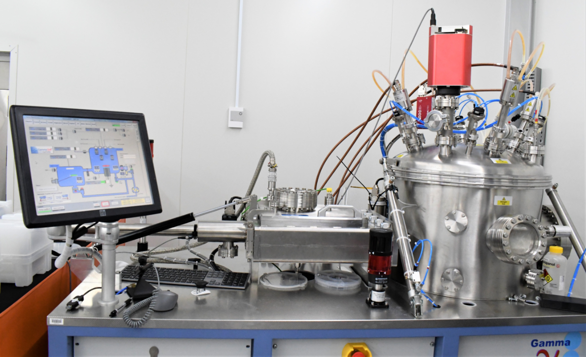
The SNS Magnetron Sputterer is a physical vapour deposition system designed for high-quality deposition of thin films. The machine has 4 magnetron targets, and able to perform both non-reactive and reactive sputtering with reactive nitrogen and oxygen gases, enabling repeatable thin films deposition for a wide range of material systems.
Example of use
Metals, alloys, semiconductor, and dielectric compounds (multiple target options available)
Purpose
To sputter uniform metallic and dielectric layers under controlled plasma conditions.
Material systems
- Metals, alloys, and dielectric compounds (multiple target options available)
- New materials avaialble on request
Scale/volume
Able to hold froma small fragment to 6-inch wafer
Specification/Resolution
Deposition rate: typical 0.1 – 10 Å/s
Reactive sputtering with oxygen/nitrogen gas available
Multiple target holders (DC/RF magnetron configuration)
Substrate temperature control up to 400°C
Base pressure: typical 10⁻8 mbar
Model
Surrey NanoSystems Gamma 1000C Confocal magnetron sputterer
Site
Griffith University
Location
Cleanroom, QMF, N74 (Bldg N74), Nathan Campus
Instrument contact
Atomic Layer Deposition (ALD)
Atomic Layer Deposition (ALD) is an advanced thin-film coating and surface processing technique. It
enables the precise and repeatable deposition of ultra-thin films, including oxides, nitrides, sulfides,
carbides, fluorides, metals, and even polymers, on virtually any surface. ALD ensures exceptional
control over film thickness, uniformity, composition, and conformality, producing films that are inherently
pinhole-free, crack-free, and defect-free. The process operates in a vacuum at relatively low
temperatures, making it suitable for coating sensitive surfaces.

Scale/volume:
Single wafer processing maximum 6 inch circular.
Capabilities:
Maximum 150 mm (6 inch) diameter circular substrate size with substrate heating up to
650 deg Celsius.
Thermal ALD with deposition temperatures up to 500 deg Celsius.
Plasma ALD with plasms power 100 W to 3000 W and frequency 1.7 to 3 MHz.
Semiautomatic substrate loader.
PicoflowTM diffusion enhancer for structures with high aspect ratio. [** PicoflowTM must
be operated with thermal lid only]
Precursor gases – oxygen (O2), ammonia (NH3), Nitrogen (N2), Argon (Ar)
Typical processes – Al2O3, TiO2, SiO2, Nb2O5, SiN, TiN, AlN, SiON (check with ANFFQld for other material processes).
Model:
Site:
The University of Queensland
Location:
Room 238, L2 ANFFQ cleanroom, AIBN (Bldg #75), St Lucia


